Nielson Scientific
  • Home
  • Products/Case Studies
    • Probe Cards
    • Terahertz Filters
    • Superconducting Cables
    • Micro Metal Mesh
  • Our Capabilities
    • 3D Semiconductor Etching
    • Nano Ablation
    • Light Assisted Wire EDM
  • Micro 3D Blog
  • Jobs
  • Contact Us
  • More
    • Home
    • Products/Case Studies
      • Probe Cards
      • Terahertz Filters
      • Superconducting Cables
      • Micro Metal Mesh
    • Our Capabilities
      • 3D Semiconductor Etching
      • Nano Ablation
      • Light Assisted Wire EDM
    • Micro 3D Blog
    • Jobs
    • Contact Us
Nielson Scientific
  • Home
  • Products/Case Studies
    • Probe Cards
    • Terahertz Filters
    • Superconducting Cables
    • Micro Metal Mesh
  • Our Capabilities
    • 3D Semiconductor Etching
    • Nano Ablation
    • Light Assisted Wire EDM
  • Micro 3D Blog
  • Jobs
  • Contact Us

Welcome

At Nielson Scientific, we design and build semiconductor solutions

At Nielson Scientific, we design and build semiconductor solutionsAt Nielson Scientific, we design and build semiconductor solutionsAt Nielson Scientific, we design and build semiconductor solutions

Our engineers and scientists are dedicated to solving your microsystem challenges

Learn More

Our Story

Dr. Gregory Nielson founded Nielson Scientific with a goal of advancing microfabrication beyond the limits of traditional 2D lithography. After completing a PhD at MIT in micro and nanotechnology, Greg took a position at Sandia National Laboratories first as a Truman Fellow and then as a Member of the Technical Staff designing and fabricating microsystems for applications including advanced solar power, high-precision navigation, silicon photonics for data networking, and advanced sensors and optical and thermal detectors. During this time, Dr. Nielson became frustrated by the limits that 2D lithography and related traditional microfabrication capabilities place on microsystem designs and recognized the remarkable potential that a true 3D microfabrication capability held.


In 2017, after a successful tenure as Chief Scientist at Vivint Solar, Greg launched Nielson Scientific. Since that time he and his team of highly skilled engineers and scientists have developed advanced 3D microfabrication capabilities for semiconductors, metals, and other materials. The team at Nielson Scientific has used these new capabilities to solve microsystem challenges for a variety of private and public customers. Our team is passionate about using cutting-edge technology and innovative techniques to bring innovation to the world of microsystems. 


We love challenges and would love to make your microsystem challenge the inspiration for the next "impossible" microdevice we build. Please contact us with your project to create something extraordinary.
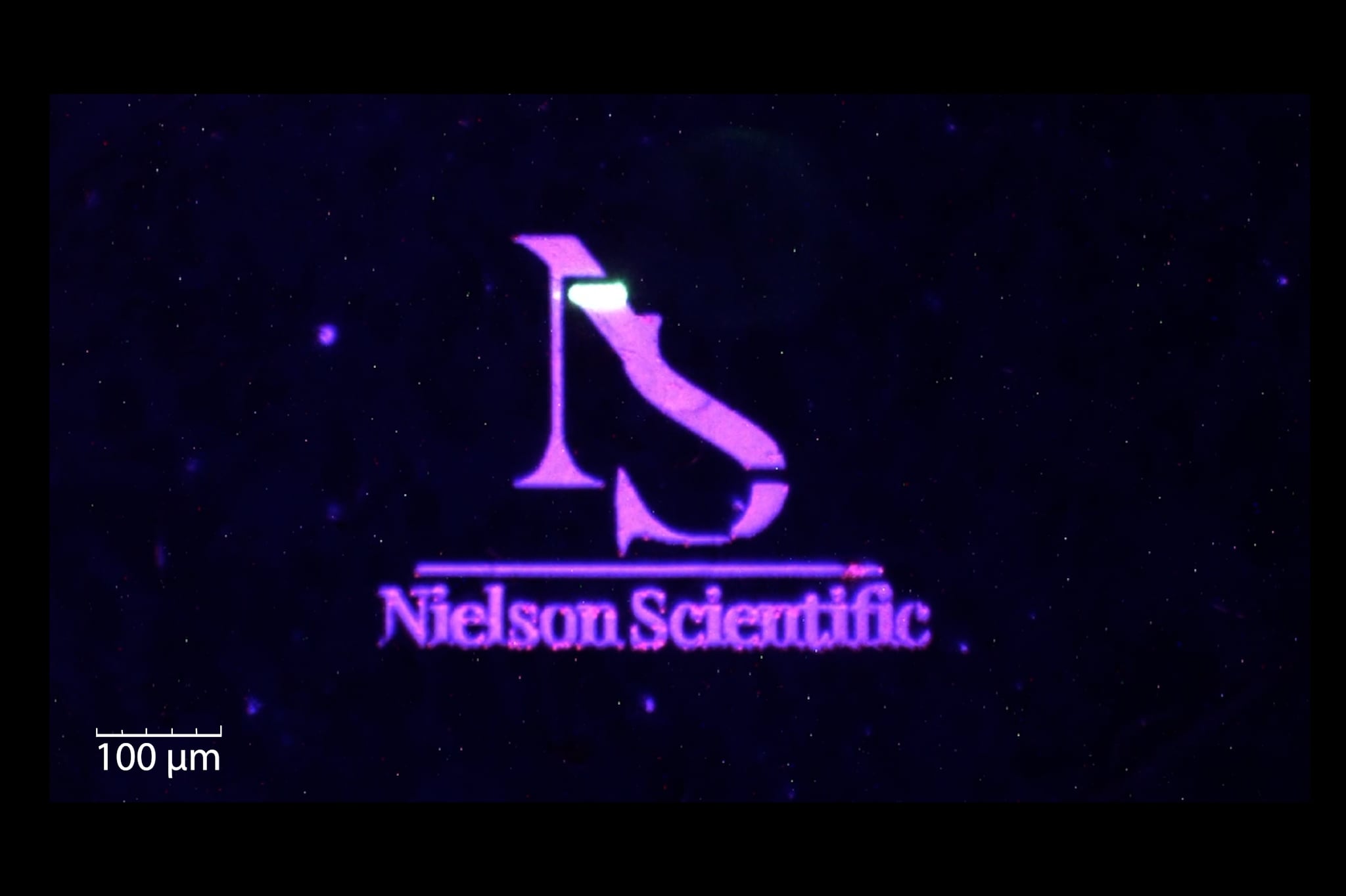
Our Capabilities

Proprietary Microfabrication Capabilities

We have developed multiple proprietary fabrication technologies to address the needs of our customers. These techniques include:

  • a direct-write 3D etching technology.  for high-quality single-crystal semiconductor materials that can create non-line-of-sight, high aspect ratio (>100:1) features down to a resolution of a few microns, 
  • a direct-write nano-ablation technology that can create feature sizes down to below one micron with positioning resolution of 50 nm on non-planar surfaces. With precise control over pulsed laser power, we can selectively remove thin film metal layers down to 100 nm.
  • a semiconductor wire electrical discharge machining (EDM) process that creates fast, precise, low kerf loss cuts in semiconductor materials with feature sizes in the tens of microns.

Conventional Fabrication Capabilities

We employ a full-range of traditional microfabrication capabilities to complement our proprietary microfabrication methods including thin-film deposition of various materials, lithography, and wet and dry etching. We also use rapid prototyping tools (3D printers and CNC machine tools) to create macro-scale components for both customer deliveries and to support our internal tool development.

Advanced Metrology

To characterize the complex 3D microstructures we fabricate, we use a variety of tools including optical and electron microscopy, 3D micro-CT scanning, confocal optical imaging systems, and other imaging and electronic test capabilities. 

Advanced Microsystem Design

The team at Nielson Scientific has many years of experience in the design of microsystems for applications ranging from advanced detectors and sensors to thermal imaging, navigation, and advanced solar cells. Capabilities include thermal, mechanical, optical, and electrical simulation and analysis as well as 3D CAD design and 2D lithography mask layout.

Our results

    Our Core Values

    Respect

    We respect our co-workers, customers, vendors, partners, and ourselves. We demonstrate our respect through our interactions, decisions, and behaviors.  

    Integrity

    We conduct our work with integrity. We are accurate in our communications. We do the right thing. If we make a mistake, we strive to make it right.  

    Service

    We actively seek opportunities to go the extra mile to serve our co-workers, customers, vendors, and partners. 

    Solutions

    Our work creates value. We strive to clearly understand our customers' challenges and work hard to provide solutions that delight them. We use the same approach for deliveries to co-workers, partners, and vendors. 

    Contact Us

    Nielson Scientific

    (385) 743-1119 info@nielsonscientific.com

    Get in Touch

    This site is protected by reCAPTCHA and the Google Privacy Policy and Terms of Service apply.

    Cancel

    Industry and Company News


    Copyright © 2023 Nielson Scientific LLC - All Rights Reserved.

    This website uses cookies.

    We use cookies to analyze website traffic and optimize your website experience. By accepting our use of cookies, your data will be aggregated with all other user data.

    Accept